

Bare Metal STM32 - GPIO
Peeling back the layers of abstraction, we have bare-metal programming for microcontrollers. One thing I think many students don’t learn during university is how to actually use official documentation (e.g. datasheets). So I wanted to create a short guide on how I go about performing common tasks using bare-metal programming on the STM32F411. I’ll be using STM32CubeIDE, but feel free to use any IDE you like.
Setup
We will reference three pieces of documentation:
I will also be including these headers into my project.
- CMSIS (Common Microcontroller Software Interface Standard) headers provided by ARM.
stm32f411xe.hheader provided by ST
ARM designs the CPU architecture and licenses it to manufacturers like STMicroelectronics to build chips around. The CMSIS headers define the Cortex-M4 core, and they’re wired up to the STM32F411’s peripherals via stm32f4xx.h, which is what we’ll actually be including.
To include the headers into the project:
Right-click your project → Properties → C/C++ Build → Settings → MCU GCC Compiler → Include Paths. Hit the ”+” icon and add the paths
So in my case I would be adding the following paths:
Headers/CMSISandHEADERS/ST
Blinking an LED
The User Manual tells us that the green user LED (LD2) is connected to PA5 (Port A, Pin 5):
User LD2: the green LED is a user LED connected to … STM32 I/O PA5 (pin 21) …
Enabling Clock Access to Port A
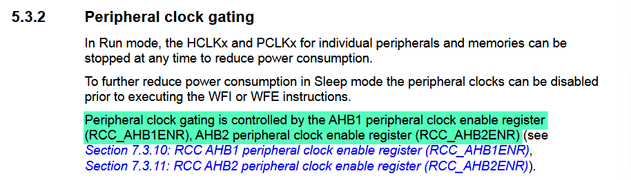
Before we can control any peripheral, we need to enable its clock. Section 5.3.2 of the Reference Manual explains that peripheral clocks are gated off by default to save power, so we need to explicitly turn them on.
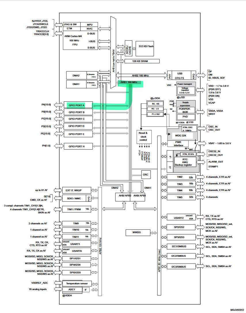
Next, we need to figure out which clock register to use: RCC_AHB1ENR or RCC_AHB2ENR. Looking at Figure 3 (STM32F411xC/xE block diagram) in the Datasheet, we can see that GPIO Port A sits on the AHB1 bus (Advanced High-performance Bus), so we’ll be using RCC_AHB1ENR.
The Reference Manual covers this register in section 7.3.10 - RCC AHB1 peripheral clock enable register (RCC_AHB1ENR). To enable the clock for Port A, we set bit 0 to 1:
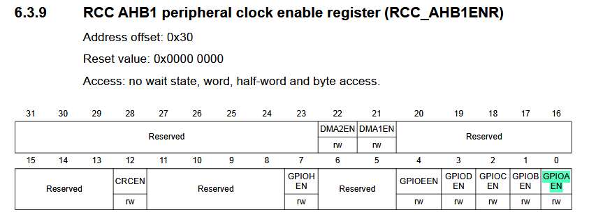
#define GPIOAEN (1U<<0)
RCC->AHB1ENR |= GPIOAEN;
Configuring Pin 5 as Output
GPIO ports have at least two registers: a direction register and a data register. The direction register configures pins as input or output; the data register reads from or writes to them.
Section 8.4.1 - GPIO Port Mode Register (GPIOx_MODER) in the Reference Manual is what we want. Each pin gets a 2-bit field, and the formula for finding pin y’s bits is 2y and 2y+1. For pin 5, that’s bits 10 and 11. The encoding for general-purpose output is 01, so right to left, bit 10 = 1 and bit 11 = 0:
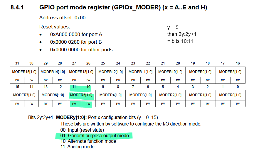
GPIOA->MODER |= (1U<<10); GPIOA->MODER &= ~(1U<<11);Toggling LED
Now that pin direction is set, we write to the data register. Section 8.4.6 - GPIO Port Output Data Register (GPIOx_ODR) in the Reference Manual covers this. We can toggle pin 5 by XOR-ing its bit on every iteration:
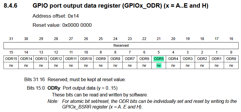
We can toggle Pin5 by inverting the bit every time:
#define PIN5 (1U<<5)
GPIOA->ODR ^= PIN5;
Putting it all together
#include "stm32f4xx.h"
#define GPIOAEN (1U<<0)#define PIN5 (1U<<5)
int main(void){  RCC->AHB1ENR |= GPIOAEN;  GPIOA->MODER |= (1U<<10);  GPIOA->MODER &= ~(1U<<11);
  while(1)  {    GPIOA->ODR ^= PIN5;
    // short delay    for(int i=0; i<100000; i++){};  }}
Bonus: using the BSRR
The bit set/reset register (BSRR) is used to give you atomic control over ODR pins. It’s a 32 bit register split into two halves. The the lower half is to set pins 0-15, and the upper half is to reset pins 0-15. The key advantage over the regular ODR pins is atomicity. When you do ODR ^ PIN5 that performs a read, modify, and a write. If an interrupt fires during this process, it could corrupt the state. With BSRR, the hardware handles it.
Section 8.4.7. in the Reference Manual describes this register.
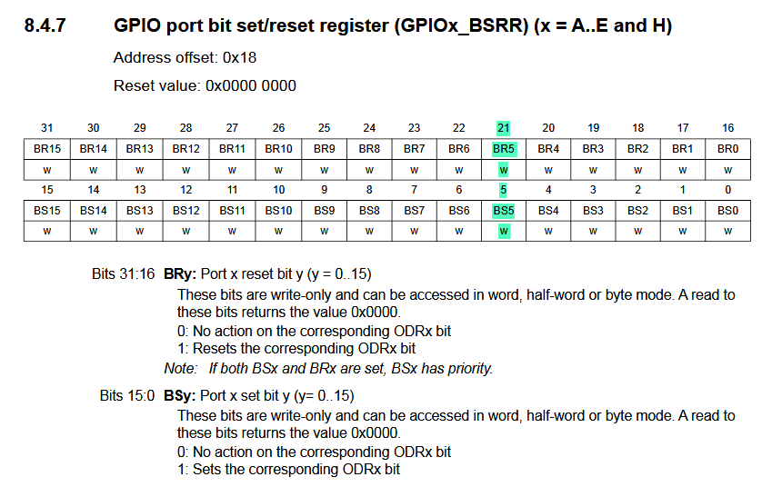
There is only a slight change to the previous program:
#include "stm32f4xx.h"
#define GPIOAEN (1U<<0)#define PIN5_SET (1U<<5)#define PIN5_RESET (1U<<21)
int main(void){  RCC->AHB1ENR |= GPIOAEN;  GPIOA->MODER |= (1U<<10);  GPIOA->MODER &= ~(1U<<11);
  while(1)  {    GPIOA->BSRR = PIN5_SET;    for(int i=0; i<100000; i++){};
    GPIOA->BSRR = PIN5_RESET;    for(int i=0; i<100000; i++){};  }
}
Using a button as an input
Found once again in the Reference Sheet, the input register is very simple:
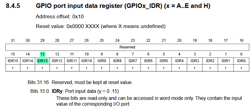
Suppose we connect a button to pin 13. Then we can read it’s state like so:
#define BTN_PIN (1U<<13)
if (GPIOC->IDR & BTN_PIN)
Our final program now looks like:
#include "stm32f4xx.h"
#define GPIOAEN (1U<<0)#define GPIOCEN (2U<<0)#define PIN5_SET (1U<<5)#define PIN5_RESET (1U<<21)#define BTN_PIN (1U<<13)

int main(void){
// Enable clock access to GPIOsRCC->AHB1ENR |= GPIOAEN;RCC->AHB1ENR |= GPIOCEN;
// Set PA5 as output pin (LED)GPIOA->MODER |= (1U<<10);GPIOA->MODER &= ~(1U<<11);
// Set PC13 as input pin (Button)GPIOC->MODER &= ~(1U<<26);GPIOC->MODER &= ~(1U<<27);
  while(1)  {    // Check if the button is pressed    if (GPIOC->IDR & BTN_PIN)    {      GPIOA->BSRR = PIN5_SET; // Turn on LED    }    else    {      GPIOA->BSRR = PIN5_RESET; // Turn off LED    }  }}
← Back to blog